Diamonds power semiconductor testing, while quantum microscopes reveal current pathways in real time.
Release date:
2025-08-04
In integrated circuit manufacturing and quality control, visualizing the internal current distribution has long been a technological bottleneck. Traditional electrical probe methods not only fail to provide a comprehensive view of internal current paths but can also potentially damage sensitive components. Recently, an Indian research team leveraged quantum Diamond The Quantum Diamond Microscope (QDM) has successfully demonstrated high-precision current imaging in wafer-scale amorphous indium-gallium-zinc oxide (a-IGZO) thin-film transistor circuits, offering a new approach for non-destructive testing and performance optimization of flexible electronic devices.
The research team includes Mayana Yousuf Ali Khan, Pralekh Dubey, and Phani Kumar Peddibothla from the Indian Institute of Science Education and Research, Bhopal (IISER Bhopal), as well as Lakshmi Madhuri P, Ashutosh Kumar Tripathi, and Pydi Ganga Bahubalindruni from the Indian Institute of Technology Kanpur (IIT Kanpur). They detailed this groundbreaking research in their recently published paper titled "Sensing Electric Currents in an a-IGZO TFT-Based Circuit Using a Quantum Diamond Microscope."

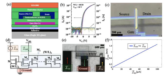
The team fabricated a current mirror circuit consisting of 16 transistors based on a-IGZO thin-film transistors (TFTs), and then used QDM at the wafer level to perform magnetic field imaging, allowing them to reconstruct the current distribution. The results show:
QDM's measured current density distribution closely matches that of conventional electrical testing.
Capable of revealing current paths that cannot be directly accessed by conventional probe methods;
High-precision characterization of circuit operating states was achieved without any physical contact with the circuit.
Technical Principles and Advantages
QDM operates based on the magnetic-field sensitivity of nitrogen-vacancy (NV) centers in diamonds. NV centers are quantum defects in the diamond lattice, formed when a nitrogen atom substitutes for a carbon atom, accompanied by a nearby vacancy. Their unique quantum mechanical properties make them highly sensitive to even the weakest magnetic fields.
When a direct current flows through a circuit, it generates a magnetic field. The QDM can capture the distribution of these magnetic fields and produce a two-dimensional magnetic field image. Researchers then further process this magnetic field data to derive the current density distribution, enabling them to visualize the internal current flow paths within the device. Importantly, this method is entirely non-invasive, meaning it neither damages nor alters the device being tested.
Compared to traditional electrical probes, QDM offers the following advantages:
Non-contact measurement, preventing damage to sensitive structures;
Uncover hidden current paths to enhance diagnostic accuracy;
It features high quantitative accuracy and closely matches the results of conventional electrical tests.
Research Background and Development
The principle of NV-center magnetic field measurement was established as early as the studies by Gruber et al. (1997) and Doherty et al. (2013), and its potential in the field of nanoscale magnetic sensing has been repeatedly validated. Subsequent research—including work by Reuss, Nomura, Roth, Tetienne, Broadway, Abrahams, and others—has continuously advanced the technology by improving sensitivity, spatial resolution, and expanding its application scenarios, thereby laying a robust foundation for the development of QDM.
This study applies QDM to a-IGZO TFT circuit imaging, representing a significant practical application of the technology in flexible electronics testing and validating its promising potential for quality control in next-generation semiconductor materials.
The study demonstrates that QDM's highly sensitive imaging capability for current distribution can be used to:
Process Optimization: Helping engineers identify and eliminate defects in the manufacturing process;
Flexible Electronics Quality Control: Providing Non-Destructive Testing for Emerging Material Devices such as a-IGZO;
Performance Evaluation: Precisely analyzing the relationship between current paths and device performance.
In the future, the research team plans to extend QDM to more complex integrated circuits and explore real-time current monitoring and 3D imaging capabilities. This will provide richer data support for chip-level diagnostics, defect tracking, and design optimization.
The quantum diamond microscope, leveraging NV-center magnetic field imaging, enables non-contact, high-precision measurements of current distribution and has successfully demonstrated wafer-level verification in a-IGZO TFT circuits. This breakthrough not only provides a reliable, non-destructive inspection method for flexible electronics manufacturing but also paves the way for enhanced quality control and design optimization in the semiconductor industry. As imaging technology and data analysis techniques continue to advance, QDM is poised to become an indispensable tool in the research and production processes of cutting-edge electronic devices.
Previous page
Previous page
Latest News
Latest News
Get a Free Consultation
If you're interested in our products, please contact us today for more detailed information.

Liaocheng Xinko Pyrophyllite Co., Ltd. is a company specializing in the professional manufacturing and processing of products such as automatic four-column hydraulic presses, diamond synthesis components, pyrophyllite stones, magnesia rings/cups, and graphite tubes.
Liaocheng High-Tech Industrial Development Zone, Bayiliang Village, North End, Jiuzhou Subdistrict Office


 2026-01-09

